11 minutes
SAP 1: Building an 8-bit FPGA computer
I’m just beginning to get into FPGAs and recently came across this : SAP-1 Implementation Project. It follows this book called Digital Computer Electronics which lays the design for what it calls Simple-as-possible (SAP) Computer. There are 3 parts to this starting with the incredibly simple SAP-1 to the final version SAP-3. I don’t have an actual physical FPGA yet so I’m just using vivado to get the simulation.
Overview
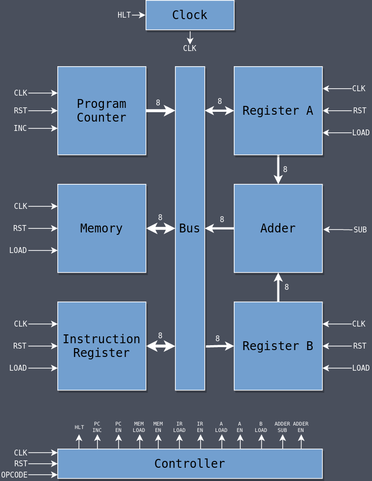
Most of the modules share common signals like : clk, rst and out
- clk: The clock signal which coordinates everything.
- rst: The reset signal which resets everything back to zero.
- out: The output of each module which is later connected to the bus.
Modules
Clock
The clock module has 2 inputs : clk_in and hlt. The hlt signal is later used as part of the SIG_HLT instruction to stop the clock from ticking and halt the computer execution.
module clock(
	input hlt, // halt signal
	input clk_in,

	output clk_out
);

	assign clk_out = hlt ? 1'b0 : clk_in;

endmodule
Program counter
The program counter keeps track of the address of the next instruction to be executed in the sequence of a program’s instructions. It counts from 0x0 to 0xF as there’s only 16 bytes of memory in this computer. If the clock goes high and inc is asserted, the value in the PC is incremented by one, otherwise it stays the same.
module pc(
	input clk,
	input rst,
	input inc,

	output[7:0] out
);

	reg[3:0] pc;

	always @ (posedge clk, posedge rst)
	begin
		if (rst)
		begin
			pc <= 4'b0;
		end else if (inc)
		begin
			pc <= pc + 1;
		end
	end

	assign out = pc;

endmodule
Instruction Register
The instruction register holds the current instruction that is to be executed. After the instruction is fetched from memory, it is loaded into the instruction register. Once the instruction is in the IR, it is decoded to understand what actions need to be performed. This involves interpreting the opcode (operation code) and any operands specified in the instruction. This will be done in the controller module.
module ir(
	input clk,
	input rst,
	input load,
	input[7:0] bus,

	output[7:0] out
);

reg[7:0] ir;

always @ (posedge clk, posedge rst)
begin
    if (rst)
    begin
        ir <= 8'b0;
    end else if (load)
    begin
        ir <= bus;
    end
end

assign out = ir;

endmodule
Memory
The Memory Address Register (MAR) is 4-bits long and is used to store a memory address. This stored address is sent to the RAM where data and instructions are read from. It takes the computer 2 cycles to read from memory: 1st cycle will load an address from the bus into the MAR and the second cycle uses the value in the MAR to address into ram and output that value onto the bus. This computer will initialize the memory by loading from a file called program.bin.
module memory(
	input clk,
	input rst,
	input load,
	input[7:0] bus,

	output[7:0] out
);

	// setting memory
	initial begin
		$readmemh("program.bin", ram);
	end

	reg[3:0] mar;
	reg[7:0] ram[0:15];		// 16 8-bit wide elements

	always @ (posedge clk, posedge rst)
	begin
		if (rst)
		begin
			mar <= 4'b0;
		end else if (load)
		begin
			mar <= bus[3:0];
		end
	end

	assign out = ram[mar];

endmodule
Register A (Accumulator)
This is the main register of the computer which stores the intermediate data during an execution. bus is an input which is driven by some other module and Register A can read from it when it needs to load which happens when load is asserted.
module reg_a(
	input clk,
	input rst,
	input load,
	input[7:0] bus,

	output[7:0] out
);

reg[7:0] reg_a;

always @ (posedge clk, posedge rst)
begin
    if (rst)
    begin
        reg_a <= 8'b0;
    end else if (load)
    begin
        reg_a <= bus;
    end
end

assign out = reg_a;

endmodule
Register B
Register B is identical to Register A in design but it never drives the bus directly; its output is fed to the Adder only. The SAP-1 is designed so that Register A is where the main action occurs and Register B supports it.
module reg_b(
	input clk,
	input rst,
	input load,
	input[7:0] bus,

	output[7:0] out
);

reg[7:0] reg_b;

always @ (posedge clk, posedge rst)
begin
    if (rst)
    begin
        reg_b <= 8'b0;
    end else if (load)
    begin
        reg_b <= bus;
    end
end

assign out = reg_b;

endmodule
Adder
The SAP-1 can only do addition and subtraction. The two registers (A and B) are where all of the math operations occur: A + B or A - B. The adder is constantly calculating either addition or subtraction based on the values in a and b and being placed directly onto its output out.
module adder(
	input[7:0] a,
	input[7:0] b,
	input sub,

	output[7:0] out
);

	assign out = sub ? (a - b): (a + b);

endmodule
Controller
This is the trickiest part of the whole computer. It decides what the computer will do next by asserting the different control signals that have gone into each of the modules.
Those control signals are:
- SIG_HLT - Halt execution of the computer
- SIG_PC_INC - Increment the Program Counter
- SIG_PC_EN - Put the value in the Program Counter onto the bus
- SIG_MEM_LOAD - Load an address into the Memory Address Register
- SIG_MEM_EN - Put a value from memory onto the bus
- SIG_IR_LOAD - Load a value from the bus into the Instruction Register
- SIG_IR_EN - Put the value in the Instruction Register onto the bus
- SIG_A_LOAD - Load a value from the bus into A
- SIG_A_EN - Put the value in A onto the bus
- SIG_B_LOAD - Load a value from the bus into B
- SIG_ADDER_SUB - Subtract the value in B from A
- SIG_ADDER_EN - Put the adder’s value onto the bus
The opcode is passed from the IR into the controller module to do different things based on what instruction is currently executing. The SAP-1 has four operations that it can perform:
- [0000] LDA $X - Load the value at memory location $X into A.
- [0001] ADD $X - Add the value at memory location $X to A and store the sum in A.
- [0010] SUB $X - Subtract the value at memory location $X from A and store the difference in A.
- [1111] HLT - Halt execution of the program.
The values in the brackets represent the opcode and all but HLT have an operand. LDA, for example, has the opcode 0000 and its operand is the address of the value to be loaded into A.
Instruction execution occurs in a series of stages where each stage takes one clock cycle. The SAP-1 has six stages, starting at Stage 0 and counting to Stage 5, at which point it returns back to Stage 0 again. This is handled by the 3-bit stage register. The stages include:
- Stage 0
- Load PC onto the bus (SIG_PC_EN)
- Load that value in memory (SIG_MEM_LOAD)
- Stage 1
- Increment PC (SIG_PC_INC)
- Stage 2
- Load memory onto bus (SIG_MEM_EN)
- Load bus into IR (SIG_IR_LOAD)
After the first three stages, the actions performed during the next three differ depending on the instruction.
- LDA
- Stage 3
- Load operand onto bus (SIG_IR_EN)
- Load value into memory, at the MAR address (SIG_MEM_LOAD)
- Stage 4
- Load that MAR address onto the bus (SIG_MEM_EN)
- Load that value in Register A (SIG_A_LOAD)
- Stage 5 -Idle
- Stage 3
- ADD
- Stage 3
- Load operand onto bus (SIG_IR_EN)
- Load value into memory, at the MAR address (SIG_MEM_LOAD)
- Stage 4
- Load that MAR address onto the bus (SIG_MEM_EN)
- Load that value in Register B (SIG_B_LOAD)
- Stage 5
- Load value in adder onto bus (SIG_ADDER_EN)
- Load the value back in Register A (SIG_A_LOAD)
- Stage 3
- SUB
- Stage 3
- Load operand onto bus (SIG_IR_EN)
- Load value into memory, at the MAR address (SIG_MEM_LOAD)
- Stage 4
- Load that MAR address onto the bus (SIG_MEM_EN)
- Load that value in Register B (SIG_B_LOAD)
- Stage 5
- Do subtraction (SIG_ADDER_SUB)
- Load value in adder onto bus (SIG_ADDER_EN)
- Load the value back in Register A (SIG_A_LOAD)
- Stage 3
- HLT
- Stage 3
- Halt the clock
- Stage 4
- Idle
- Stage 5
- Idle
- Stage 3
module controller(
    input clk,
    input rst,
    input [3:0] opcode,
    output [11:0] out,
    output reg [2:0] stage  // Expose stage as output
);

localparam SIG_HLT_VALUE       = 11;
localparam SIG_PC_INC_VALUE    = 10;
localparam SIG_PC_EN_VALUE     = 9;
localparam SIG_MEM_LOAD_VALUE  = 8;
localparam SIG_MEM_EN_VALUE    = 7;
localparam SIG_IR_LOAD_VALUE   = 6;
localparam SIG_IR_EN_VALUE     = 5;
localparam SIG_A_LOAD_VALUE    = 4;
localparam SIG_A_EN_VALUE      = 3;
localparam SIG_B_LOAD_VALUE    = 2;
localparam SIG_ADDER_SUB_VALUE = 1;
localparam SIG_ADDER_EN_VALUE  = 0;

localparam OP_LDA = 4'b0000;
localparam OP_ADD = 4'b0001;
localparam OP_SUB = 4'b0010;
localparam OP_HLT = 4'b1111;

reg [11:0] ctrl_word;

always @(posedge clk or posedge rst) begin
    if (rst) begin
        stage <= 0;
    end else begin
        if (stage == 5) begin
            stage <= 0;
        end else begin
            stage <= stage + 1;
        end
    end
end

always @(*) begin
    ctrl_word = 12'b0;

    case (stage)
        0: begin
            ctrl_word[SIG_PC_EN_VALUE] = 1;
            ctrl_word[SIG_MEM_LOAD_VALUE] = 1;
        end
        1: begin
            ctrl_word[SIG_PC_INC_VALUE] = 1;
        end
        2: begin
            ctrl_word[SIG_MEM_EN_VALUE] = 1;
            ctrl_word[SIG_IR_LOAD_VALUE] = 1;
        end
        3: begin
            case (opcode)
                OP_LDA: begin
                    ctrl_word[SIG_IR_EN_VALUE] = 1;
                    ctrl_word[SIG_MEM_LOAD_VALUE] = 1;
                end
                OP_ADD: begin
                    ctrl_word[SIG_IR_EN_VALUE] = 1;
                    ctrl_word[SIG_MEM_LOAD_VALUE] = 1;
                end
                OP_SUB: begin
                    ctrl_word[SIG_IR_EN_VALUE] = 1;
                    ctrl_word[SIG_MEM_LOAD_VALUE] = 1;
                end
                OP_HLT: begin
                    ctrl_word[SIG_HLT_VALUE] = 1;
                end
            endcase
        end
        4: begin
            case (opcode)
                OP_LDA: begin
                    ctrl_word[SIG_MEM_EN_VALUE] = 1;
                    ctrl_word[SIG_A_LOAD_VALUE] = 1;
                end
                OP_ADD: begin
                    ctrl_word[SIG_MEM_EN_VALUE] = 1;
                    ctrl_word[SIG_B_LOAD_VALUE] = 1;
                end
                OP_SUB: begin
                    ctrl_word[SIG_MEM_EN_VALUE] = 1;
                    ctrl_word[SIG_B_LOAD_VALUE] = 1;
                end
            endcase
        end
        5: begin
            case (opcode)
                OP_ADD: begin
                    ctrl_word[SIG_ADDER_EN_VALUE] = 1;
                    ctrl_word[SIG_A_LOAD_VALUE] = 1;
                end
                OP_SUB: begin
                    ctrl_word[SIG_ADDER_SUB_VALUE] = 1;
                    ctrl_word[SIG_ADDER_EN_VALUE] = 1;
                    ctrl_word[SIG_A_LOAD_VALUE] = 1;
                end
            endcase
        end
    endcase
end

assign out = ctrl_word;


endmodule
Top module
Instantiate all the modules and make sure the connections between them are correctly established:
module top (
    input CLK,
    input rst
);

wire hlt;
wire clk;
reg [7:0] bus;
wire [7:0] pc_out;
wire [7:0] ir_out;
wire [7:0] reg_a_out;
wire [7:0] reg_b_out;
wire [7:0] adder_out;
wire [7:0] memory_out;
wire [3:0] opcode;
wire[11:0] ctrl_word;
wire inc;
wire load;
wire load_a;
wire load_b;
wire sub;
wire memory_load;
wire [2:0] stage;

always @(*) begin
	if (ctrl_word[5]) begin
		bus = ir_out;
	end else if (ctrl_word[0]) begin
		bus = adder_out;
	end else if (ctrl_word[3]) begin
		bus = reg_a_out;
	end else if (ctrl_word[7]) begin
		bus = memory_out;
	end else if (ctrl_word[9]) begin
		bus = pc_out;
	end else begin
		bus = 8'b0;
	end
end

clock clock_inst (
    .hlt(ctrl_word[11]),
    .clk_in(CLK),
    .clk_out(clk)
);


pc pc_inst (
    .clk(clk),
    .rst(rst),
    .inc(ctrl_word[10]),
    .out(pc_out)
);


ir ir_inst (
    .clk(clk),
    .rst(rst),
    .load(ctrl_word[6]),
    .bus(bus),
    .out(ir_out)
);


reg_a reg_a_inst (
    .clk(clk),
    .rst(rst),
    .load(ctrl_word[4]),
    .bus(bus),
    .out(reg_a_out)
);

reg_b reg_b_inst (
    .clk(clk),
    .rst(rst),
    .load(ctrl_word[2]),
    .bus(bus),
    .out(reg_b_out)
);


adder adder_inst (
    .a(reg_a_out),
    .b(reg_b_out),
    .sub(ctrl_word[1]),
    .out(adder_out)
);


memory memory_inst (
    .clk(clk),
    .rst(rst),
    .load(ctrl_word[8]),
    .bus(bus),
    .out(memory_out)
);


controller controller_inst (
    .clk(clk),
    .rst(rst),
    .opcode(ir_out[7:4]),
    .out(ctrl_word),
    .stage(stage)

);

assign hlt = ctrl_word[11];
assign inc = ctrl_word[10];
assign load = ctrl_word[6];
assign load_a = ctrl_word[4];
assign load_b = ctrl_word[2];
assign sub = ctrl_word[1];
assign memory_load = ctrl_word[8];

endmodule
Simulation
module testbench();

    reg CLK;
    reg rst;
    wire hlt;
    wire clk;
    wire [7:0] pc_out;
    wire [7:0] ir_out;
    wire [7:0] reg_a_out;
    wire [7:0] reg_b_out;
    wire load_b;
    wire load_a;
    wire [7:0] adder_out;
    wire [7:0] memory_out;
    wire [3:0] opcode;
    wire [11:0] ctrl_word;
    wire [2:0] stage;


    top uut (
        .CLK(CLK),
        .rst(rst)
    );
    wire[4:0] bus_en = {ctrl_word[9],ctrl_word[7],ctrl_word[5],ctrl_word[3],ctrl_word[0]};
    reg[7:0] bus;

    always @(*) begin
        case (bus_en)
            5'b00001: bus = adder_out;
            5'b00010: bus = reg_a_out;
            5'b00100: bus = ir_out;
            5'b01000: bus = memory_out;
            5'b10000: bus = pc_out;
            default: bus = 8'b0;
        endcase
    end

    // Generate clock signal
    integer i;
    initial begin
        CLK = 0;
        for (i = 0; i < 128; i=i+1) begin
            #1 CLK = ~CLK;
        end
    end

    // Test sequence
    initial begin
        // Initialize signals
        rst = 1;
        #10 rst = 0;

        // Monitor signals
        $monitor("Time: %0t | CLK: %b | rst: %b | hlt: %b | opcode: %b | ctrl_word: %b | pc_out: %h | ir_out: %h | reg_a_out: %b | reg_b_out: %b | adder_out: %h | memory_out: %h",
                 $time, CLK, rst, hlt, opcode, ctrl_word, pc_out, ir_out, reg_a_out, reg_b_out, adder_out, memory_out);


        // Wait for the system to stabilize
        #100;

        #200 $finish;
    end


assign clk = uut.clock_inst.clk_out;
assign hlt = uut.clock_inst.hlt;

assign pc_out = uut.pc_out;
assign ir_out = uut.ir_out;
assign memory_out = uut.memory_out;

assign reg_a_out = uut.reg_a_out;
assign reg_b_out = uut.reg_b_out;
assign adder_out = uut.adder_out;

assign load_a = uut.reg_a_inst.load;
assign load_b = uut.reg_b_inst.load;

assign opcode = uut.controller_inst.opcode;
assign ctrl_word = uut.controller_inst.out;
assign stage = uut.stage;


endmodule
To program the computer, we can program the bytes directly into a file named program.bin. This file will get loaded into the memory module when the computer starts. Here is the annotated test program (program.bin):
$0 |   0D  // LDA [$D]   Load A with the value at address $D
$1 |   1E  // ADD [$E]   Add the value at address $E to A
$2 |   2F  // SUB [$F]   Subtract the value at address $F from A
$3 |   F0  // HLT        Stop execution
$4 |   00
$5 |   00
$6 |   00
$7 |   00
$8 |   00
$9 |   00
$A |   00
$B |   00
$C |   00
$D |   03  // Data: 3
$E |   04  // Data: 4
$F |   02  // Data: 2
And here is the simulation (Satisfying ngl) :
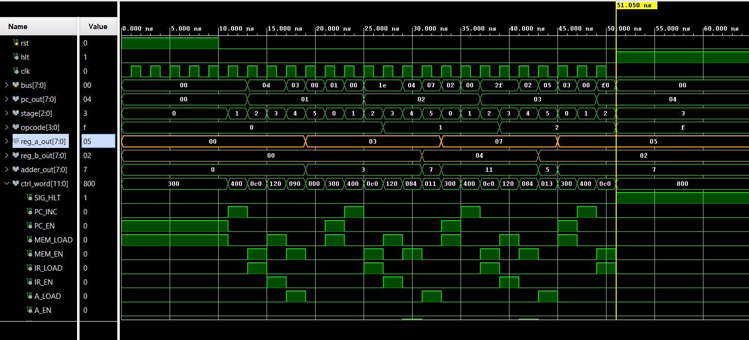
The yellow signals show the values of reg_a and reg_b You can see the values of reg_a changing to 3 + 4 - 2 = 5 and then then hlt signal causes the clk to stop ticking.